- 您现在的位置:买卖IC网 > Sheet目录3840 > PIC18F6410-I/PT (Microchip Technology)IC PIC MCU FLASH 8KX16 64TQFP
2010 Microchip Technology Inc.
DS39635C-page 21
PIC18F6310/6410/8310/8410
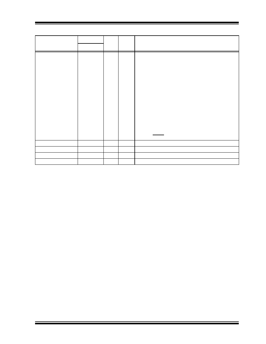
PORTG is a bidirectional I/O port.
RG0/CCP3
RG0
CCP3
3
I/O
ST
Digital I/O.
Capture 3 input/Compare 3 output/PWM3 output.
RG1/TX2/CK2
RG1
TX2
CK2
4
I/O
O
I/O
ST
—
ST
Digital I/O.
AUSART2 asynchronous transmit.
AUSART2 synchronous clock (see related RX2/DT2).
RG2/RX2/DT2
RG2
RX2
DT2
5
I/O
I
I/O
ST
Digital I/O.
AUSART2 asynchronous receive.
AUSART2 synchronous data (see related TX2/CK2).
RG3
6
I/O
ST
Digital I/O.
RG4
8
I/O
ST
Digital I/O.
RG5
See RG5/MCLR/VPP pin.
VSS
9, 25, 41, 56
P
—
Ground reference for logic and I/O pins.
VDD
10, 26, 38, 57
P
—
Positive supply for logic and I/O pins.
AVSS
20
P
—
Ground reference for analog modules.
AVDD
19
P
—
Positive supply for analog modules.
TABLE 1-2:
PIC18F6310/6410 PINOUT I/O DESCRIPTIONS (CONTINUED)
Pin Name
Pin Number
Pin
Type
Buffer
Type
Description
TQFP
Legend:
TTL = TTL compatible input
CMOS = CMOS compatible input or output
ST = Schmitt Trigger input with CMOS levels
Analog = Analog input
I
= Input
O
= Output
P= Power
I2C = ST with I2C or SMB levels
Note 1:
Default assignment for CCP2 when Configuration bit, CCP2MX, is set.
2:
Alternate assignment for CCP2 when Configuration bit, CCP2MX, is cleared.
发布紧急采购,3分钟左右您将得到回复。
相关PDF资料
200346-2
CONN HOUSING RECEPT 20POS BLACK
PIC16F84A-20/P
IC MCU FLASH 1KX14 EE 18DIP
200838-2
CONN HOUSING RECEPT 34POS BLACK
PIC18LF2420-I/SO
IC MCU FLASH 8KX16 28SOIC
5172625-3
CONN RCPT HSNG 24POS BLUE PNL MT
202758-1
CONN HOUSING PLUG 6POS BLACK
TS80C31X2-VIC
IC MCU 8BIT 40/30MHZ 44-PQFP
TS80C31X2-MCC
IC MCU 8BIT 40/20MHZ 44-PQFP
相关代理商/技术参数
PIC18F6410-I/PT
制造商:Microchip Technology Inc 功能描述:IC 8BIT FLASH MCU 18F6410 TQFP64
PIC18F6410T-I/PT
功能描述:8位微控制器 -MCU 16kBF 768RM 68I/O RoHS:否 制造商:Silicon Labs 核心:8051 处理器系列:C8051F39x 数据总线宽度:8 bit 最大时钟频率:50 MHz 程序存储器大小:16 KB 数据 RAM 大小:1 KB 片上 ADC:Yes 工作电源电压:1.8 V to 3.6 V 工作温度范围:- 40 C to + 105 C 封装 / 箱体:QFN-20 安装风格:SMD/SMT
PIC18F6490-E/PT
功能描述:8位微控制器 -MCU 16kBF 768RM 68I/O RoHS:否 制造商:Silicon Labs 核心:8051 处理器系列:C8051F39x 数据总线宽度:8 bit 最大时钟频率:50 MHz 程序存储器大小:16 KB 数据 RAM 大小:1 KB 片上 ADC:Yes 工作电源电压:1.8 V to 3.6 V 工作温度范围:- 40 C to + 105 C 封装 / 箱体:QFN-20 安装风格:SMD/SMT
PIC18F6490-I/PT
功能描述:8位微控制器 -MCU 16kBF 768RM 68I/O RoHS:否 制造商:Silicon Labs 核心:8051 处理器系列:C8051F39x 数据总线宽度:8 bit 最大时钟频率:50 MHz 程序存储器大小:16 KB 数据 RAM 大小:1 KB 片上 ADC:Yes 工作电源电压:1.8 V to 3.6 V 工作温度范围:- 40 C to + 105 C 封装 / 箱体:QFN-20 安装风格:SMD/SMT
PIC18F6490-I/PT
制造商:Microchip Technology Inc 功能描述:IC 8BIT FLASH MCU 18F6490 TQFP64
PIC18F6490-I/PT
制造商:Microchip Technology Inc 功能描述:8 BIT MICROCONTROLLER CLOCK SPEED:40MHZ
PIC18F6490T-I/PT
功能描述:8位微控制器 -MCU 16kBF 768RM 68I/O RoHS:否 制造商:Silicon Labs 核心:8051 处理器系列:C8051F39x 数据总线宽度:8 bit 最大时钟频率:50 MHz 程序存储器大小:16 KB 数据 RAM 大小:1 KB 片上 ADC:Yes 工作电源电压:1.8 V to 3.6 V 工作温度范围:- 40 C to + 105 C 封装 / 箱体:QFN-20 安装风格:SMD/SMT
PIC18F6493-I/PT
功能描述:8位微控制器 -MCU 128 Segmnt LCD DRVR 12B ADC 16KB 768BRAM RoHS:否 制造商:Silicon Labs 核心:8051 处理器系列:C8051F39x 数据总线宽度:8 bit 最大时钟频率:50 MHz 程序存储器大小:16 KB 数据 RAM 大小:1 KB 片上 ADC:Yes 工作电源电压:1.8 V to 3.6 V 工作温度范围:- 40 C to + 105 C 封装 / 箱体:QFN-20 安装风格:SMD/SMT